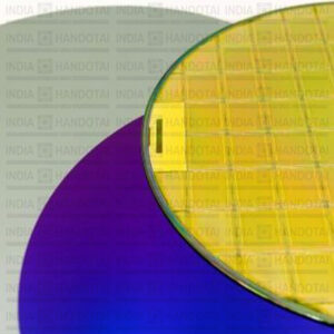


India Handotai supplies an extensive range of compound semiconductor wafer materials, so called because they are made of two or more elements, including Silicon Carbide (SiC), Gallium Nitride (GaN), Gallium Arsenide (GaAs) and Indium Phosphide (InP) to the research, development and production sectors.
GaN can be supplied as single crystal wafers or GaN templates on Sapphire wafers. The latter is more commonly used as the costs are lower and there is more flexibility on dopants. Fe doped Semi insulating, undoped N type and Si doped N type are readily available on short lead-times, with diameters of 50 mm, 100 mm and 150 mm and GaN thicknesses of 2, 4 and up to 20 um.
GaN on SiC wafers are also available and offer exceptionally low switching losses in IGBT applications such as EV’s and other high power applications where the excellent thermal stability of SiC results in well managed losses and good reliability.
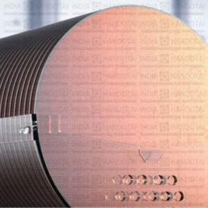
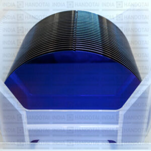
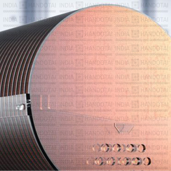
SiC wafers are used widely for EPI layer growth and are grown by a seeded sublimation process. All grades are available in any quantity and with short lead-times. Our SiC wafers come with a unique laser marked ID in the backside (C terminated face) of the wafer.
GaAs, InP, and a range of other III-V compound semiconductor wafers are also available in small quantities and on short lead-times. Doped semiconducting or semi insulating wafers in inventory and wafers are shipped in single wafer shipper storage boxes to maintain integrity of ID and also avoid damage during storage.
Further information about semiconductor wafer properties can be found in our “Wafer Selection Guide“, knowledge base document.
Compound semiconductor wafers can be ordered directly with Inseto, or purchased via our online store. The web-store also includes a list of our current inventory, which is available for rapid shipment worldwide and silicon wafer price information that registered users can view.
Please do not hesitate to contact our application and technical specialists for advice, or if you need assistance specifying wafers for your requirement.
Product Range Overview
More about our Sapphire wafers:
- Sapphire Wafer sizes from 2” to 150mm, from inventory
- Very high quality low defectivity and tight TTV and flatness
- High purity 99.998%
- Single and double sided polished available
- C, A, and R plane orientations
- Small lot sizes and Laser marking of wafers available
- Short lead-time for delivery
Applications
Deep Etched Devices and Membranes, Critical Lithography, Wafer Bonding, Stepper Qualification, EPI Growth, IR detectors and THz Devices, Graphene Research, Power Electronics, Medical Devices, CMOS, Microfluidics, MEMS Devices, Sensors, Renewable, Energy Harvesting, Equipment Setup and Verification etc.
Industry Segments
Semiconductor & Related Research and Manufacturing, Coating Development, Adhesion Testing etc.
Region
Available Worldwide from India Handotai