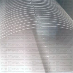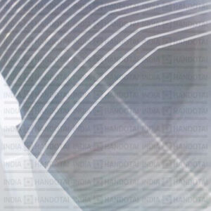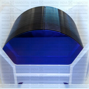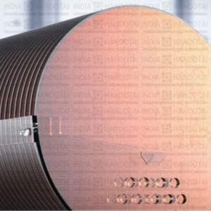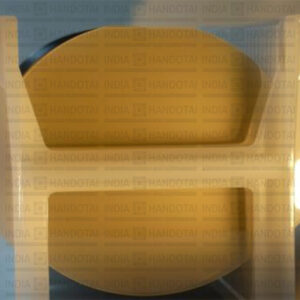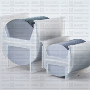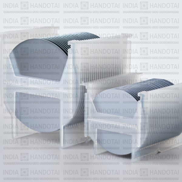


India Handotai supplies and stocks an extensive range of high-quality virgin Silicon Wafer from 25-300mmm (1-12”) in diameter, in various resistivity’s, orientations and thicknesses.
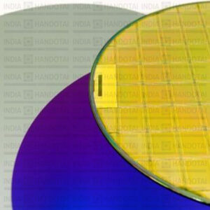
The wafers are ideal substrates for research applications, setup and tool qualification of precision equipment (e.g. steppers & other fabrication processes) and semiconductor production requirements. Silicon is exceptionally flat, hard and has very tight thickness, TTV and other dimensional tolerances as well as being bio compatible and radiation hard.
Wafers are shipped and used worldwide by a wide range of universities, institutes, equipment vendors and leading semiconductor device manufacturers.
Silicon (Si) types include Czochralski- (CZ) or Float-Zone (FZ) grown, P-Type, N-Type or Intrinsic, etched, single (SSP) or double side polished (DSP). Tight tolerance wafers enable a range of technologies such as Si membranes Si sensors and Si detectors for pressure measurement and MEMS devices such as Si cantilevers for measurement, micro-mechanisms used in energy harvesting, substrates for energy storage, microfluidics including PCR devices, air speed measurement and ultra-precision micro-flow measurements.
Precise conductivity control allows research in 2D materials and cryogenic conductivity measurements in the few Kelvin range. With ability to stack layers easily, Si is key to enabling photonic devices and integrated photonics used in optical interconnects and quantum devices.
Further information about semiconductor wafer properties can be found in our “Wafer Selection Guide“, knowledge base document.
Silicon wafers can be ordered directly with Inseto, or purchased via our online store. The web-store also includes a list of our current inventory, which is available for rapid shipment worldwide and silicon wafer price information that registered users can view.
Please do not hesitate to contact our application and technical specialists for advice, or if you need assistance specifying wafers for your requirement.
Product Range Overview
Silicon Wafer Properties:
- Sizes: Available from 1 inch to 300mm in diameter (custom sizes also available)
- Grades: Prime, Test, and Mechanical
- Crystal Growth Methods: Czochralski (CZ) and Float Zone (FZ)
- Types: N-type, P-type, and Intrinsic (undoped) silicon
- Crystal Orientation: <100>, <110>, and <111> Miller indices
- Surface Finish: Single Side Polished (SSP) or Double Side Polished (DSP)
- Thickness: From 240 to 5000 microns, with custom options available
- Resistivity: Ranges from 0.01 to 5000 ohm·cm
- Dopants:
- N-type: Phosphorus, Arsenic, or Antimony
- P-type: Boron or Gallium
- Standards: SEMI standard PRIME and non-standard thicknesses
- Identification: Flats or notches indicate the crystallographic orientation

Applications
Deep Etched Devices and Membranes, Critical Lithography, Wafer Bonding, Stepper Qualification, EPI Growth, IR detectors and THz Devices, Graphene Research, Power Electronics, Medical Devices, CMOS, Microfluidics, MEMS Devices, Sensors, Renewable, Energy Harvesting, Equipment Setup and Verification etc.
Industry Segments
Semiconductor & Related Research and Manufacturing, Coating Development, Adhesion Testing etc.
Region
Available Worldwide from India Handotai