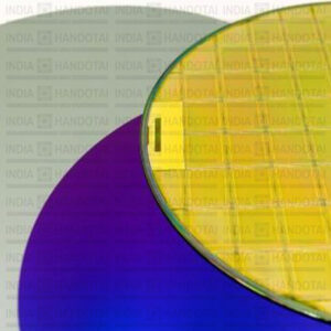
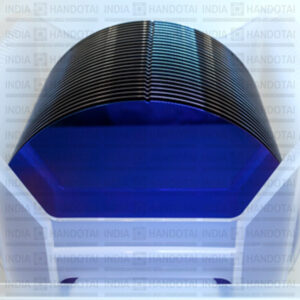
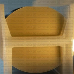
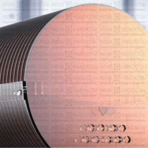
India Handotai is a specialist supplier of Bonded Silicon-on-Insulator – SOI wafers, with device layer thickness of >1.5um and exceptional device layer TTV and flatness. Our SOI wafers sizes vary from 3” to 200mm, can be made in short lead-times, with small lot sizes also available.
Direct Si-Si bonded wafers and Double bonded SOI are also available, along with thick device layers>300um, Box thickness 0.5-10um, and any dopant or orientation. We can also produce bonded wafers with oxide on the backside as well as laser marking on front or backside.
Our high-quality wafers are shipped and used worldwide by university, research and production customers. Please do not hesitate to contact our support team for application and technical advice, if you need assistance specifying your bonded wafers.
SOI wafers can be ordered directly with Inseto, or purchased via our online store. The web store also includes a list of our current inventory, which is available for rapid shipment and SOI wafer prices that registered user’s access.
Product Range Overview
More about our silicon on insulator wafers:
- SOI Wafer sizes from 3” to 200mm, some in inventory
- Very high quality with tight TTV on device layer thickness
- Direct Si-Si bonding and double sided SOI available
- Any Si orientation, any device thickness over 1.5um
- Single and double side polished
- Small lot sizes and Laser marking of wafers available
- Short lead time delivery

Applications
Graphene, Power Electronics, Medical Devices, CMOS, Microfluidics, MEMS Devices, Sensors, Renewable, Energy Harvesting etc.
Industry Segments
Semiconductor & Related Research and Manufacturing, Coating Development, Adhesion Testing etc.
Region
Available Worldwide from India Handotai