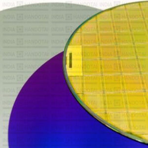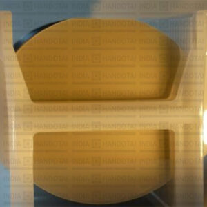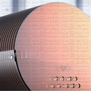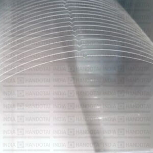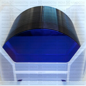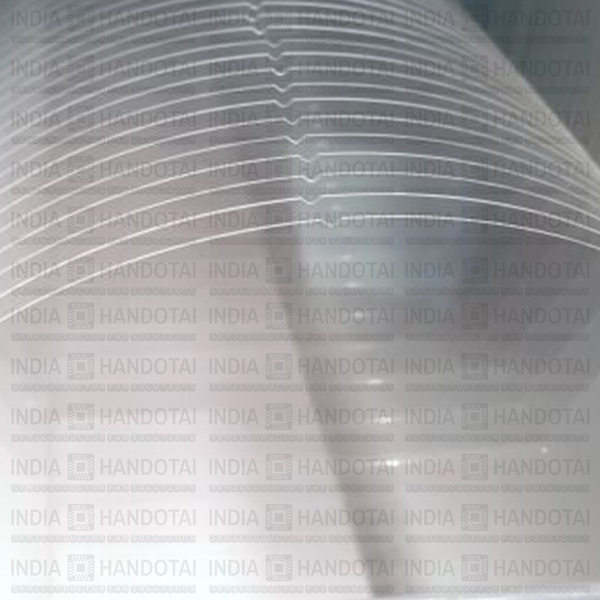

India Handotai specialize in supplying Kr grown Sapphire wafer with exceptional purity and very good surface finish, TTV, and flatness. Sapphire Wafer sizes from 2” to 150mm can be made in short lead-times and small lot sizes are also available.
Sapphire wafers are used extensively for HB-LED production due to the good lattice match between III-V and II-VI materials and Sapphire. It also has high resistance to thermal shock and can produce low stress layers.
Sapphire is also a good substrate for Si EPI growth due to very low defectivity and low loss properties. It is also widely used in the fabrication of high voltage power and frequency devices where the thermal conductance, very stable dielectric constant, and low loss properties enable it to operate reliably in very harsh conditions. It also has high optical transmission across a wide range of wavelengths.
Our high-quality Sapphire Wafers are shipped and used worldwide by University and Industrial Research, Manufacturing and equipment manufacturers. Sapphire wafers can be purchased online via the India handotai.
Please do not hesitate to contact our support team for sapphire wafer prices or technical advice, if you need assistance specifying wafers for your application.
Product Range Overview
More about our Sapphire wafers:
- Sapphire Wafer sizes from 2” to 150mm, from inventory
- Very high quality low defectivity and tight TTV and flatness
- High purity 99.998%
- Single and double sided polished available
- C, A, and R plane orientations
- Small lot sizes and Laser marking of wafers available
- Short lead-time for delivery

Applications
Optoelectronics, Photonics, Medical Devices, Microfluidics, MEMS Devices, Sensors, Renewable, Energy Harvesting, Micro-Machining etc.
Industry Segments
Semiconductor & Related Research and Manufacturing, Coating Development, Adhesion Testing etc.
Region
Available Worldwide from India Handotai