Your Products
- No products in the cart.
₹0.00
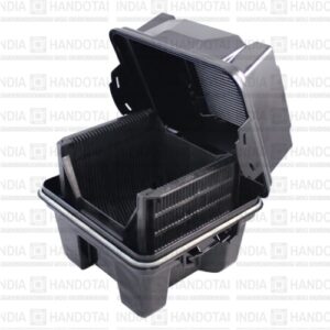
● Product name:8″ Wafer Shipping Box ESD
● Part number:SH-B200-E
● Dimension:269.0 (L) x 291.0(W) x 239.0(H)mm
● Weight:2300g
● Capacity:25 PCS
● Apply for round wafer:8 inch (Ø200mm)
● Material:PC ESD
● Slot pitch:6.35mm
● Apply for round wafer:8 inch (Ø200mm)
● Material:Metal
● Slot pitch:6.35mm
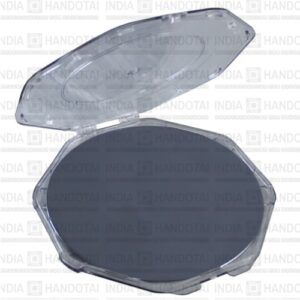
● Product name:8″ Wafer Single Tray
● Part number:SI-T200
● Dimension:228(L) x 213(W) x 21(H)mm
● Weight:258g
● Capacity:1 PCS
● Apply for round wafer:8 inch (Ø200mm)
● Material:PC/ PE / PTU
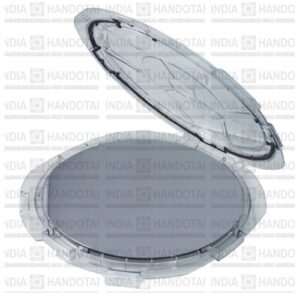
● Product name:12″ Wafer Single Tray
● Part number:SI-T300
● Dimension:356.8(L) x 343.7(W) x33.8(H)mm
● Weight:805g
● Capacity:1 PCS
● Apply for round wafer:12 inch (Ø300mm)
● Material:PC/ PE / PTU
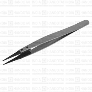
Material: Stainless Steel Antimagnetic SA
Dimensions: L 126mm
W 9mm
H 1.5mm
Tips thickness 0.5mm
Tips width 0.5mm
Net Weight: 14g
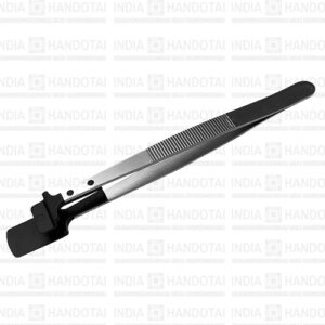
Material: Stainless Steel Antimagnetic SA
Dimensions: L 138 mm
W 10 mm
H 1.5 mm
Tips thickness 13 mm
Tips width 21 mm
Net Weight: 17g
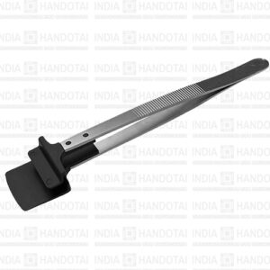
Material: Stainless Steel Antimagnetic SA
Dimensions: L 136 mm
W 10 mm
H 1.5 mm
Tips thickness 0.8 mm
Tips width 27 mm
Tips length 21mm
Net Weight: 19g
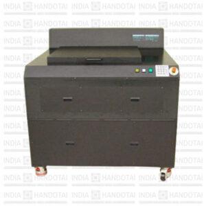
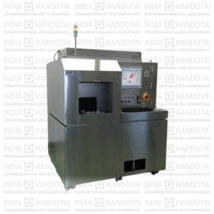
YPI – 500 – Inspection system for large glass substrate
Can inspect surface particles for large size glass substrate and film sheet.
Apply to warpage for sample center position with auto focus sensor unit.
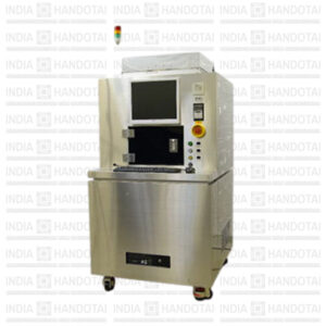
Compact・High performance Wafer surface inspection system
New designed compact and high performance of wafer surface inspection system is reduced 50% to its footprint compared with previous same kind of product. Despite compact body, the maximum sensitivity is 0.15um on bare silicon, and then it can be easy to move to your designated location with desk.
Can choose the surface isolated function (The function can measure a surface of the transparent wafer without receiving contaminations of a back wafer.) as optional for transparent substrate and wafer. Output is map, histogram, which are saved and displayed to an attached PC.

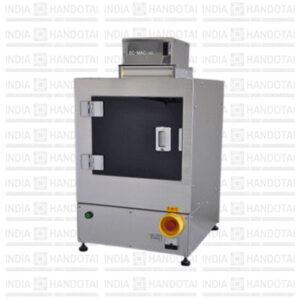
Wafer surface inspection system YPI-N series(Auto loading)
Can scan particles on mirror wafer (silicon wafer) with fast.
Wide range measurement from small size wafer (2/3inch) to 8inch wafer.
YPI – N – XY/YPI – N – Θ
Wafer surface inspection system YPI-N series(Manual)
Can scan particles on mirror wafer (silicon wafer) with fast.
Wide range measurement from small size wafer (2/3inch) to 8inch wafer.
Inspection system for film sheet which can be applied to roll to roll.
YPI-MX-XYA/YPI-MX-ΘA
Glass substrate/ Sapphire wafer surface inspection system.
YPI-MX series(Auto loading type)
Specialized to tune for a transparent substrate. Apply to measure a rough polishing of back of substrate.