Your Products
- No products in the cart.
₹0.00

Above And Beyond metrology
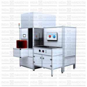
Overview, insight and outlook In one process step: What was previously unthinkable in semiconductor manufacturing, the Global Nanoscope makes measurable. The entire surface of your wafer or any reflective surface is measured completely within just 30 seconds, providing reliable nanometer-scale insights that safeguard your process chain. Whether for incoming inspection in chip manufacturing or in process control during wafer fabrication: What was previously beyond the measurable, the Global Nanoscope makes visible.
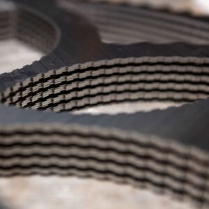
PR Hoffman is recognized as a leading innovator and manufacturer of Insert Carriers, also known as Polishing Carriers, for the semiconductor wafer industry. The insert carrier is an exclusive PR Hoffman design widely used in the semiconductor industry (and other high value wafer industries) to protect the edge profile of the wafer while providing the strength and durability of a traditional steel carrier.
Custom Designs for Semiconductor Processing
PR Hoffman generates a custom drawing for customer review and approval before any products are made. This added service ensures that our customers receive precisely the design needed for their process, on every order.
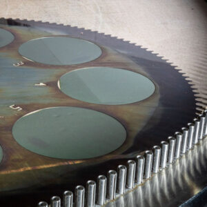
We manufacture lapping carriers (also called workholders) for planetary lapping and polishing machines including those manufactured by P.R. Hoffman, Speedfam, Peter Wolters AG, Hamai, Somos, Fujikoshi, Strausbaugh, Melchiorre, Lanzhou, Lapmaster and other specialty machines adapted for unique applications. Lapping carriers are available in a variety of materials and thicknesses, including an inventory of more than 20 spring steel thicknesses.
We can create a custom drawing that you can review to ensure the design meets your exact specifications. If you have a drawing or sample part for a lapping or polishing process, PR Hoffman can provide a detailed quotation for your review.
PR Hoffman uses a wide variety of state of the art manufacturing methods to create your lapping carriers including, precision punching, Wire-EDM cutting, CNC machining, CNC routing, and laser cutting. With these options, nearly any lapping carrier configuration is available. We will recommend the most cost-effective method based on your machine and volume requirements.
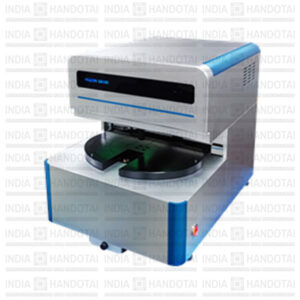
FILCON SR-300R is an R-Theta motor stage structure that can measure the thickness (t), reflectance, and transmittance of a transparent thin film of several nanometers to several tens of mm with pre-written mapping measurement recipe using vertically incident light with sub-nm precision. It is a tabletop automatic mapping spectroscopic reflection measurement equipment.
By easily creating map recipes for ~300mm wafers, you can perform thin film characteristic analysis at high speed, and measurement result display, report output, and 2D/3D graphic analysis tools are provided. It is a state-of-the-art spectroreflection measurement instrument that can be used immediately even by users without professional knowledge with a user-friendly Windows-based instrument program and an easy interface .
Application
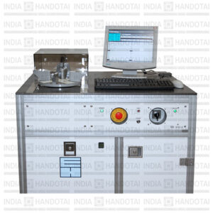
High-resolution thickness and flatness (TTV) gauge for 200–300mm silicon wafers.
Easy adaption to different thickness ranges within a few seconds. Integration into automatic robotic sorter systems possible.
The MX1012 is ideally suited for research & development, qualification of processes, and process control of thickness and flatness (TTV) especially after grinding and lapping. A pair of capacitive sensors samples four radial profiles (45 degrees) on every wafer which consist of hundreds of local thickness values. If necessary for your application, the four standard scans can be simply increased to reach an even higher measuring coverage. Comes with our powerful MX-NT operating software.
Measurement type
Thickness | Flatness (TTV)
Application
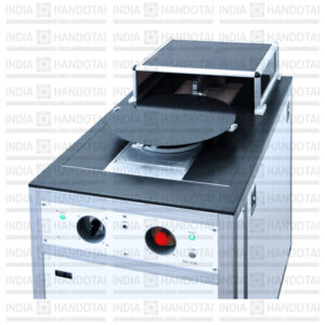
High-resolution thickness and flatness (TTV) gauge for 300–450mm silicon wafers.
Easy adaptation to different thickness ranges within a few seconds. Integration into automatic robotic sorter systems possible.
The MX1018 is ideally suited for research & development, qualification of processes, and process control of thickness and flatness (TTV).
A pair of capacitive sensors samples four radial profiles (45 degrees) on each wafer which consist of hundreds of local thickness values. If necessary for your application, the four standard scans can be simply increased to achieve an even higher measuring coverage. Comes with our powerful MX-NT operating software.
Measurement type
Thickness | Flatness (TTV)
Application
High-resolution thickness and flatness (TTV) gauge for 100–150mm silicon wafers.
Easy adaption to different thickness ranges within a few seconds. Integration into automatic robotic sorter systems possible.
The MX102-6 is ideally suited for research & development, qualification of processes, and process control of thickness and flatness (TTV). A pair of capacitive sensors samples four radial profiles (45 degrees) on every wafer.
One such profile consists of 200 local thickness values and is offset by 45 degrees relative to the neighbouring profile. Comes with our powerful MX-NT operating software.
Measurement type
Thickness | Flatness (TTV)
Application
High-resolution thickness and flatness (TTV) gauge for 150–200mm silicon wafers
Easy adaption to different thickness ranges within a few seconds. Integration into automatic robotic sorter systems possible.
The MX102-8 is ideally suited for research & development, qualification of processes, and process control of thickness and flatness (TTV).
A pair of capacitive sensors samples four radial profiles (45 degrees) on every wafer. One such profile consists of 200 local thickness
values and is offset by 45 degrees relative to the neighbouring profile. Comes with our powerful MX-NT operating software.
Measurement type
Thickness | Flatness (TTV)
Application
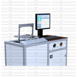
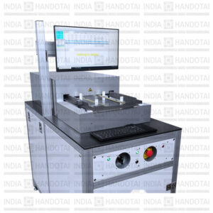
High precision chip production geometry gauge for 300mm silicon wafers.
The MX2012 works as manually loaded stand-alone station with a throughput of at least 50 wafers per hour. With its 69 measuring points it controls thickness, bow and warp in high resolution. Wafer stress evaluation is optionally available. Upright position measuring avoids gravity-induced sag. System can be converted for 200mm wafer measuring. Comes with our powerful MX-NT operating software.
Measurement type
Thickness | Flatness (TTV)
Application
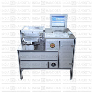
Fast chip production geometry gauge for 300mm silicon wafers.
The MX2012-H works as manually loaded stand-alone station with a throughput of at least 50 wafers per hour. With its 69 measuring points it controls thickness, bow and warp in high resolution. Wafer stress evaluation is optionally available. System can be converted for 200mm wafer measuring. Comes with our powerful MX-NT operating software.
Measurement type
Thickness | Flatness (TTV)
Application
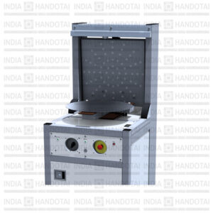
Automatable geometry gauge for thin and standard 200mm or 300mm silicon wafers.
The MX2013 works as semi-automated stand-alone station. With its 37 measuring points it gauges 300mm wafers within 50 seconds. It controls thickness, bow and warp in high resolution (Corresponds with Sori). System optional available for 200mm wafer measuring. Comes with our powerful MX-NT operating Software.
Measurement type
Thickness | Flatness (TTV)
Application
Automatable bow and warp gauge for 450mm silicon wafers.
The MX2018-W manages the difficult 450mm size wafers. Upright position measuring avoids the otherwise enormous gravity-induced sag. With its 73 measuring points it controls center thickness, bow and warp in high resolution. For covering all geometry properies we recommend using MX2018-W in combination with MX1018. Within a robot sorter these both modules can measure two wafers simultaneously without detraction of the throughput. Comes with our powerful MX-NT operating software.
Measurement type
Thickness | Flatness (TTV)