Transparent wafer, silicon wafer or LT wafer can be measured by YPI-MX-θDC. Maximum sensitivity is 0.1μm.s
")
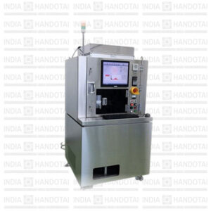
Dual Laser Units
")
Inspection Result Images
")
MAP Result for LT Wafers
| Scanning method | Rotation or XY scanning with dual laser units |
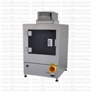
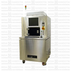
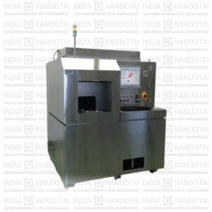
| Work piece setting | Manual or Auto loading (Cassette to Cassette) |
| Electric consumption | AC100V/200V 30A |
| Maximum sensitivity | 0.1μm |
| Reproducibility | σ/X ≦10% |
| Inspection time | Within 2 minutes for 4inch wafer |
| Target substrate and wafer | SiC wafer, GaN wafer, LT wafer, film deposited wafer, Transparent substrate and wafer |
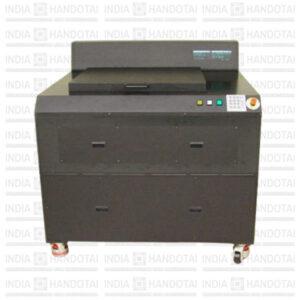
| Appearance Dimension | W900 mm×D1,000 mm×H1,757 mm(Manual) W1,530 mm×D1,200 mm×H1,715 mm(Auto loading) |
| Weight | Approx.500 Kg(Manual) Approx.1000 Kg(Auto loading) |