| Workpiece size | Maximum 200×200 mm, φ 200 mm (Apply to measure 300mm※1) |
| Maximum sensitivity (Bare Si PSL) |
Si wafer Transparent substrate (Require optional selection) |
| Scanning method | XY or Rotation scanning |
| Workpiece load | Manual |
| Dimension | W548×D572×H962 (mm) PC is separate placement |
| Weight | 90 Kg (PC is separate placement) |
| Power supply | AC 100V 15A |

Roll over image to zoom in
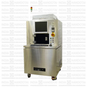
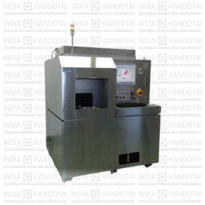
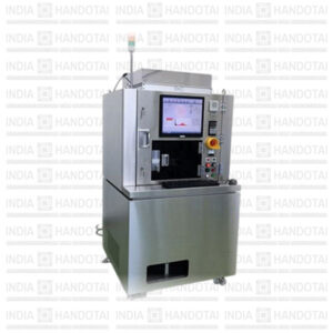
YPI – MN
Compact・High performance Wafer surface inspection system
New designed compact and high performance of wafer surface inspection system is reduced 50% to its footprint compared with previous same kind of product. Despite compact body, the maximum sensitivity is 0.15um on bare silicon, and then it can be easy to move to your designated location with desk.
Can choose the surface isolated function (The function can measure a surface of the transparent wafer without receiving contaminations of a back wafer.) as optional for transparent substrate and wafer. Output is map, histogram, which are saved and displayed to an attached PC.