Your Products
- No products in the cart.
₹0.00
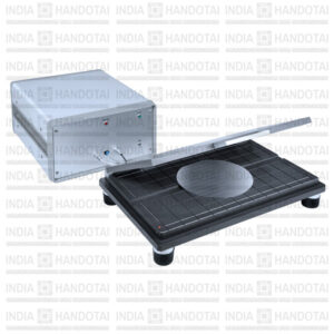
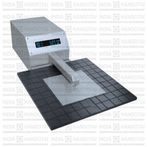
Application
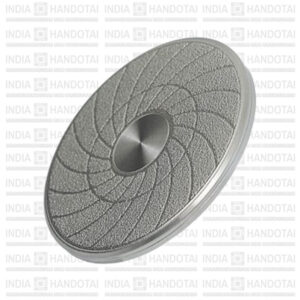
Easy one-point thickness gauge for thin, framed 200mm and 300mm silicon wafers.
The MX3012 is a robust and stable instrument for quick and simple manual thickness gauge. Especially for thin wafers, unframed and framed with dicing tape or backgrind tape. Simple handling without the tape thickness nor the tape’s dielectric constant. Light barriers avoid mismeasurement at the edges. Fully self-calibrating without the need for gauge blocks nor reference wafers. Integrated 5-digit display. Workes as stand-alone or connected to a PC via serial interface, which allows collecting data of multiple measurements, calculating flatness (TTV), mean value or standard deviation of single wafers or of complete wafer lots.
Measurement type
Thickness
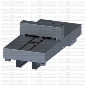
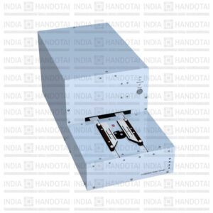
Application
The MX 302 measures a high resulution thickness scan. Prepared for integration into an automated etching system. Automatic measuring of wafers in the carrier.
Measurement type
Thickness
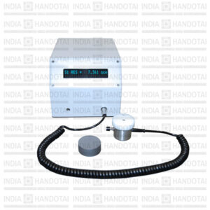
Application
Fast contactless resistivity gauge for semi-insulating wafers up to 150mm.
The MX601 gauges resistivity of wafers made of semi-insulating materials like Gallium Arsenide or Silicon Carbide. Fast handling without wafer preparation and excellent repeatability with best avoidance of piezo-electric effects. MX601’s serial interface allows data evaluation and statistics, as well as access to calibration constants and output types.
Measurement type
Thickness
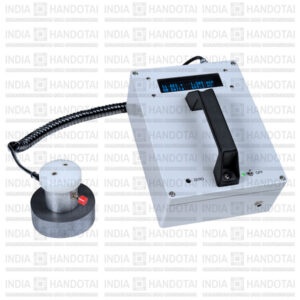
Application
Combined thickness and resistivity gauge for 200 mm and 300 mm silicon wafers.
The MX6012 is designed to characterize silicon wafers. It combines contactless thickness, resistivity and P/N dotation sensors. In addition to the center measurement, up to 15 additional points for each half scan can defined. Optionally an identical scan after 90° rotation. To be connected to a PC via serial interface. Comes with our powerful MX-NT operating software. Integration into automatic robotic sorter systems possible.
Measurement type
Thickness
Application
Fast contactless resistivity gauge for silicon blocks.
The MX604 gauges resistivity of silicon blocks of any size with the reliable eddy current method. It allows connecting up to 4
different sensor probes (alternatively) to measure different resistivity ranges. Integrated alphanumeric display. Workes as stand-alone or connected to a PC via serial interface. Our optional software EHMaster allows further evaluation of the measurements and configuration
of the tool.
Measurement type
Thickness
Application
Portable contactless resistivity gauge for silicon blocks.
The MX604-B gauges resistivity of silicon blocks of any size with the reliable eddy current method. It allows connecting up to 4 different sensor probes (alternatively) to measure different resistivity ranges. Integrated alphanumeric display. Powered by rechargable battery. With energy-saving automatic stand-by mode. Intended as portable stand-alone version of MX604.
Measurement type
Thickness
Application
Fast sheet resistance gauge for 50–200mm silicon wafers and conductive films.
The MX604-S gauges sheet resistance of semiconducting wafers and conductive films on high-ohm substrates with the reliable eddy current method. Fully self-calibrating, thus temperature and humidity changes are negligible. Integrated alphanumeric display. Workes as stand-alone or connected to a PC via serial interface, which allows collecting data of multiple measurements, mean value or standard deviation of single wafers or of complete wafer lots.
Measurement type
Thickness | Sheet resistance
Application
Combined thickness and resistivity gauge for up to 156mm solar wafers
The MX604-ST is designed to characterize solar wafers. Fits square wafers up to 156mm and round wafers from 2″ to 200mm. It combines sensors for measuring thickness and resistivity simultaneously. Fully self-calibrating, thus temperature and humidity changes are negligible. Integrated alphanumeric display. Workes as stand-alone or connected to a PC via serial interface, which allows collecting data of multiple measurements, mean value or standard deviation of single wafers or of complete wafer lots.
Measurement type
Thickness | Resistivity
Application
Combined thickness and resistivity gauge for 150mm and 200mm silicon wafers.
The MX608 is designed to characterize silicon wafers. It combines contactless thickness, resistivity and P/N dotation sensors. Automatic move-in and turn of the wafer allows up to 18 scans of each wafer. To be connected to a PC via serial interface. Comes with our powerful MX-NT operating software. Integration into automatic robotic sorter systems possible.
Measurement type
Thickness
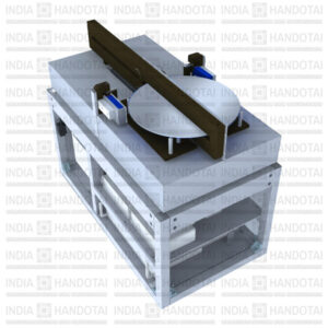
Application
High resolution thickness and surface profiler for as-sawn 450mm silicon wafers.
The MX7012 is designed to control thickness, flatness (TTV), warp, waviness and roughness after wire sawing. Capacitive sensors scan a diagonal cut through the center of the wafer. On the sides where the saw wire enters and exits, thickness and roughness are measured simultaneously. (The latter with an opto-electronic measuring system.) Available asin-line integrated module or as hand-loaded stand-alone for spot checks. Comes with our powerful MX-NT operating software.
Measurement type
Thickness
Application
The MX7018 is designed to control thickness, flatness (TTV), warp, waviness and roughness after wire sawing. Capacitive sensors scan a diagonal cut through the center of the wafer. On the sides where the saw wire enters and exits, thickness and roughness are measured simultaneously. (The latter with an opto-electronic measuring system.) Available asin-line integrated module or as hand-loaded stand-alone for spot checks. Comes with our powerful MX-NT operating software.
Measurement type
Thickness