| Wafer Diameter | 50mm, 75mm, 100mm |
| Accuracy | ±0.1 µm |
| Resolution | 0.1µm |
| Thickness range | 300 – 800 µm |
| Non-conductive substrates | yes |
| Semi-insluation materials | above 107 Ohm*cm |
| Software | MXNT |
Roll over image to zoom in
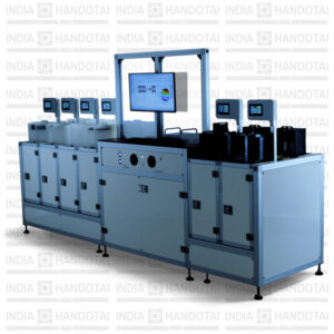
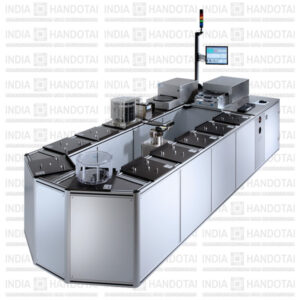
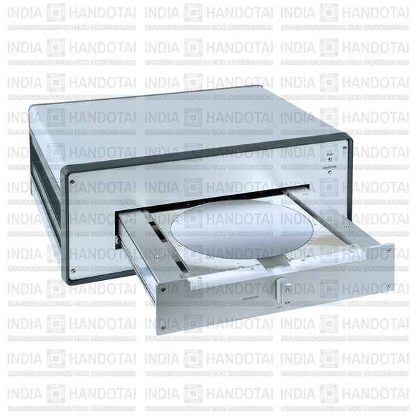
MX 203-4-37-Q
Application
Fast contactless geometry gauge for 2–4″ non-conductive and semi-insulating wafers.
High throughput: the MX203-4-37-Q gauges with its 37 measuring points every wafer within max. 10 seconds. It controls thickness and flatness. Flexible wafer size adjustment by various centering-frames. Suitable for wafers made of non-conductive substrates (Quartz, Saphire, Lithium Niobate, Lithium Tantalate) and semi-insulating materials like Gallium Arsenide or Silicon Carbide. Comes with our powerful MX-NT operating software.
Measurement type
Thickness | Flatness (TTV)