Advantages and Features

The Global Nanoscope combines innovative technology and multiple fields of application with proven benefits such as seamless integratability and excellent support.
- Full-surface measurement: An unbeatable competitive advantage for you: Stitching is a thing of the past.
- Highest speed: Within 30 seconds, the GNS measures your substrate. After 1-2 minutes you will receive your 3D evaluation of the determined data.
- True nanotopography: The GNS offers reliable nanometer height resolution for analytical purposes.
- Insensitive to vibration: Many high-precision metrology systems can only be used reliably if they are set up absolutely vibration-free. However, the GNS is robust against floor vibrations and motion disturbances of modern production environments.
- Budget-friendly: Despite high-tech, the maintenance costs of the GNS are very low and all parts are very robust and durable.
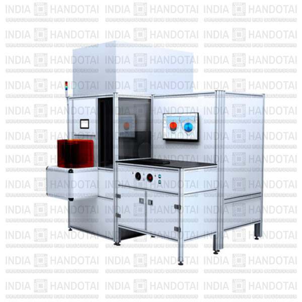
- Fully automatic & integratable: The GNS is a fully automatic measuring system and can be used in any workflow environment.
- Consulting and support: Individual planning, consulting and support are available throughout the entire service life of your GNS through us and our local distributors
Possible Applications
The application possibilities of the GNS are as comprehensive as its range of features. Let us inspire you!
- Any surface evaluation and classification is possible quickly and contact-free with the Global Nanoscope, e.g.
– Identification of dimples
– defect analysis
– Peak-to-valley analysis of surfaces - Wafer fabrication: For fast and comprehensive process control of many production steps during wafer fabrication (e.g. grinding, polishing)
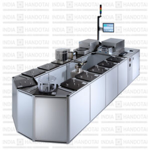
- Chip fabrication: The Global Nanoscope is particularly well suited for rapid incoming inspection of wafers to be processed.
- Analysis according to SEMI M43 Guide for Reporting Wafer Nanotopography: Determine standard-compliant detail values in the nanometer range.
- Glass & optical Industry: All reflective surfaces are suitable for nanometer precision measurement via Global Nanoscope.
The Global Nanoscope can also be used in many other industries such as medical technology, energy or research and development.
Talk to our team about your requirements!

Innovative Technology

You already know Makyoh methods? Our proprietary and AMA-approved Advanced Makyoh technology goes one step further than was previously measurable:
- India Handotai Advanced Makyoh: Conventional Makyoh systems provide two-dimensional grayscale images showing irregularities on a surface. However, the actual height of such surface structures is crucial for industrial applications, especially in sensitive processes such as wafer production. Conventional Makyoh systems therefore measure purely qualitatively: typically, standard Makyoh images are quite blurry.
- The system based on India Handotai Advanced Makyoh, however, determines real height information of the surface in one measurement process.
- Classical 2D Makyoh images in 2D are also provided by the Global Nanoscope: but with a very high resolution. Our system is therefore capable of both qualitative and quantitative measurement.
- The Advanced Makyoh image data can be further processed as desired: For inspection, for complex 3D analysis or for evaluation by existing IT landscapes and control systems.
Examples
Applications
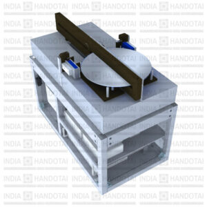
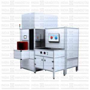
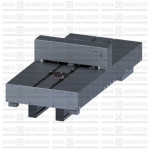
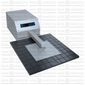
Multifunctional high-end measuring system for fast, non-contact, non-destructive, motionless measurement of all reflective surfaces up to 300mm.
Characteristics
Thickness | Flatness (TTV)
Technical Data
| Wafer diameter | up to 300 mm |
| Dynamic range | gradient: ±0.14°, bow up to 100 μm |
| Lateral resolution | 110 μm |
| Resolution (height) | 1 nm (typically, with small bow below 50 μm) |
| Standard Deviation | 1 σ ≤ 1 nm (n=31) |
| Edge Exclusion | 1mm (Notch + Mount) |
| Measuring time | 30 sec |
| Calculation time | 1 – 2 minutes |
| Vibrational stability | VC-A (~50 μm/s [4 – 80 Hz]) |
| Typical data size per Wafer | 50 MB (500 MB full analysis data) |