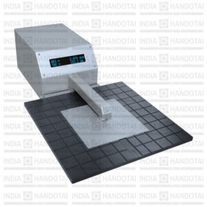
| Wafer Diameter | 300mm |
| Accuracy | ±0.5 µm |
| Resolution | 50µm |
| Thickness range | 500 – 900 µm |
| Automatic wafer geometry gauge | yes |
| Software | MXNT |
Roll over image to zoom in
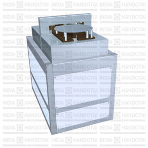
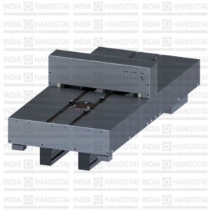
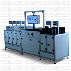
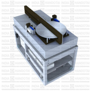
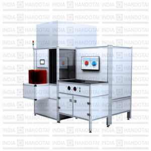
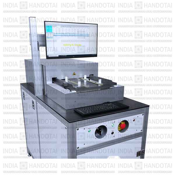
MX 2012-H
Application
Fast chip production geometry gauge for 300mm silicon wafers.
The MX2012-H works as manually loaded stand-alone station with a throughput of at least 50 wafers per hour. With its 69 measuring points it controls thickness, bow and warp in high resolution. Wafer stress evaluation is optionally available. System can be converted for 200mm wafer measuring. Comes with our powerful MX-NT operating software.
Measurement type
Thickness | Flatness (TTV)