Your Products
- No products in the cart.
₹0.00
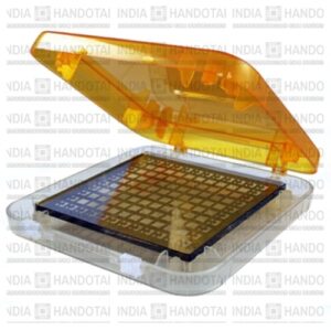
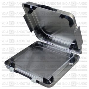
● Product name:Mask Package Box
● Part number:MS-B6025-A
● Dimension: 200(W)x218(L)x39(H)mm
● Weight:344.5g
● Capacity:1 PCS
● Mask size:6025 Mask(6 inch)
● Material:ABS
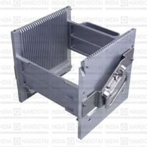
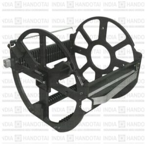
● Product name:8″ Metal Cassette
● Part number:MT-C200-A
● Dimension:214(L) x 202.7 (W) x 206 (H)mm
● Weight:3600g
● Capacity:25 PCS
● Apply for round wafer:8 inch (Ø200mm)
● Material:Metal
● Slot pitch:6.35mm
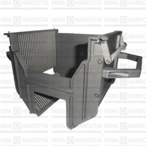
● Product name:8″ Metal Cassette
● Part number:MT-C200-B
● Dimension:205.54(L)x240(W)x218.94(H)mm
● Weight:3300g
● Capacity:25 PCS
● Apply for round wafer:8 inch (Ø200mm)
● Material:Metal
● Slot pitch:6.35mm
● Product name:12″ Metal Cassette
● Part number:MT-C300
● Dimension:380(L) x 388.8(W) x 312(H)mm
● Weight:4000g
● Capacity:25 PCS
● Apply for round wafer:12 inch (Ø300mm)
● Material:Metal
● Slot pitch:10mm
● Product name:Metal Mask Package Box
● Part number:MS-B6025-M
● Dimension:
215.85(L) x 206.36(W) x 37.82(H)mm
● Weight:566g
● Capacity:1 PCS
● Mask size:6025 Mask(6 inch)
● Material:Metal
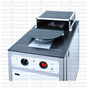
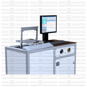
Application
High-resolution thickness and flatness (TTV) gauge for 200–300mm silicon wafers.
Easy adaption to different thickness ranges within a few seconds. Integration into automatic robotic sorter systems possible.
The MX1012 is ideally suited for research & development, qualification of processes, and process control of thickness and flatness (TTV) especially after grinding and lapping. A pair of capacitive sensors samples four radial profiles (45 degrees) on every wafer which consist of hundreds of local thickness values. If necessary for your application, the four standard scans can be simply increased to reach an even higher measuring coverage. Comes with our powerful MX-NT operating software.
Measurement type
Thickness | Flatness (TTV)
Application
High-resolution thickness and flatness (TTV) gauge for 300–450mm silicon wafers.
Easy adaptation to different thickness ranges within a few seconds. Integration into automatic robotic sorter systems possible.
The MX1018 is ideally suited for research & development, qualification of processes, and process control of thickness and flatness (TTV).
A pair of capacitive sensors samples four radial profiles (45 degrees) on each wafer which consist of hundreds of local thickness values. If necessary for your application, the four standard scans can be simply increased to achieve an even higher measuring coverage. Comes with our powerful MX-NT operating software.
Measurement type
Thickness | Flatness (TTV)
Application
High-resolution thickness and flatness (TTV) gauge for 100–150mm silicon wafers.
Easy adaption to different thickness ranges within a few seconds. Integration into automatic robotic sorter systems possible.
The MX102-6 is ideally suited for research & development, qualification of processes, and process control of thickness and flatness (TTV). A pair of capacitive sensors samples four radial profiles (45 degrees) on every wafer.
One such profile consists of 200 local thickness values and is offset by 45 degrees relative to the neighbouring profile. Comes with our powerful MX-NT operating software.
Measurement type
Thickness | Flatness (TTV)
Application
High-resolution thickness and flatness (TTV) gauge for 150–200mm silicon wafers
Easy adaption to different thickness ranges within a few seconds. Integration into automatic robotic sorter systems possible.
The MX102-8 is ideally suited for research & development, qualification of processes, and process control of thickness and flatness (TTV).
A pair of capacitive sensors samples four radial profiles (45 degrees) on every wafer. One such profile consists of 200 local thickness
values and is offset by 45 degrees relative to the neighbouring profile. Comes with our powerful MX-NT operating software.
Measurement type
Thickness | Flatness (TTV)
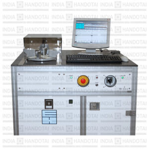
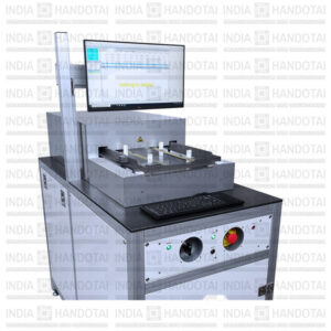
Application
High precision chip production geometry gauge for 300mm silicon wafers.
The MX2012 works as manually loaded stand-alone station with a throughput of at least 50 wafers per hour. With its 69 measuring points it controls thickness, bow and warp in high resolution. Wafer stress evaluation is optionally available. Upright position measuring avoids gravity-induced sag. System can be converted for 200mm wafer measuring. Comes with our powerful MX-NT operating software.
Measurement type
Thickness | Flatness (TTV)
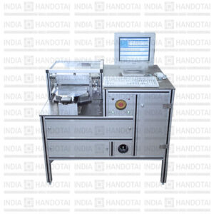
Application
Fast chip production geometry gauge for 300mm silicon wafers.
The MX2012-H works as manually loaded stand-alone station with a throughput of at least 50 wafers per hour. With its 69 measuring points it controls thickness, bow and warp in high resolution. Wafer stress evaluation is optionally available. System can be converted for 200mm wafer measuring. Comes with our powerful MX-NT operating software.
Measurement type
Thickness | Flatness (TTV)
Application
Automatable geometry gauge for thin and standard 200mm or 300mm silicon wafers.
The MX2013 works as semi-automated stand-alone station. With its 37 measuring points it gauges 300mm wafers within 50 seconds. It controls thickness, bow and warp in high resolution (Corresponds with Sori). System optional available for 200mm wafer measuring. Comes with our powerful MX-NT operating Software.
Measurement type
Thickness | Flatness (TTV)