Your Products
- No products in the cart.
₹0.00
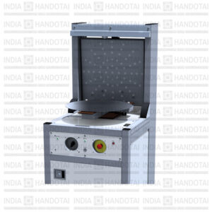
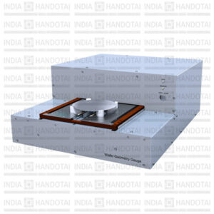
Application
Automatable bow and warp gauge for 450mm silicon wafers.
The MX2018-W manages the difficult 450mm size wafers. Upright position measuring avoids the otherwise enormous gravity-induced sag. With its 73 measuring points it controls center thickness, bow and warp in high resolution. For covering all geometry properies we recommend using MX2018-W in combination with MX1018. Within a robot sorter these both modules can measure two wafers simultaneously without detraction of the throughput. Comes with our powerful MX-NT operating software.
Measurement type
Thickness | Flatness (TTV)
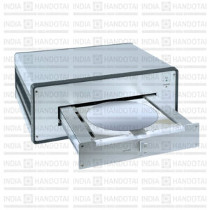
Application
Fast contactless geometry gauge for 2–4″ silicon wafers.
High throughput: the MX203-4-21 gauges with its 21 measuring points every wafer within max. 5 seconds. It controls thickness, bow and warp. Wafer stress evaluation is optionally available. Flexible wafer size adjustment by various centering-frames. Comes with our powerful MX-NT operating software.
Measurement type
Thickness | Flatness (TTV) | Bow | Warp
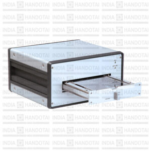
Application
Fast contactless geometry gauge for 2–4″ non-conductive and semi-insulating wafers.
High throughput: the MX203-4-37-Q gauges with its 37 measuring points every wafer within max. 10 seconds. It controls thickness and flatness. Flexible wafer size adjustment by various centering-frames. Suitable for wafers made of non-conductive substrates (Quartz, Saphire, Lithium Niobate, Lithium Tantalate) and semi-insulating materials like Gallium Arsenide or Silicon Carbide. Comes with our powerful MX-NT operating software.
Measurement type
Thickness | Flatness (TTV)
Application
Fast contactless geometry gauge for thin 125– 200mm silicon wafers.
High throughput: the MX203-58-37-B gauges with its 37 measuring points every wafer within max. 8 seconds. It controls thickness, bow and warp after back side grinding. Flexible wafer size adjustment by various centering-frames. Comes with our powerful MX-NT operating software.
Measurement type
Thickness | Flatness (TTV) | Bow | Warp
Application
Fast contactless geometry gauge for 100–150mm silicon wafers.
High throughput: the MX203-6-33 gauges with its 33 measuring points every wafer within max. 7 seconds. It controls thickness, bow and warp. Wafer stress evaluation is optionally available. Flexible wafer size adjustment by various centering-frames. Comes with our powerful MX-NT operating software.
Measurement type
Thickness | Flatness (TTV) | Bow | Warp
Application
Fast contactless geometry gauge for thin 100–150mm silicon wafers.
High throughput: the MX203-6-33-B gauges with its 33 measuring points every wafer within max. 7 seconds. It controls thickness, bow and warp after back side grinding. Flexible wafer size adjustment by various centering-frames. Comes with our powerful MX-NT operating software.
Measurement type
Thickness | Flatness (TTV) | Bow | Warp
Application
Fast contactless geometry gauge for 75–200mm non-conductive and semi-insulating wafers.
High throughput: the MX203-6-33-Q gauges with its 33 measuring points every wafer within max. 10 seconds. It controls thickness and flatness. Flexible wafer size adjustment by various centering-frames. Suitable for wafers made of non-conductive substrates (Quartz, Saphire, Lithium Niobate, Lithium Tantalate) and semi-insulating materials like Gallium Arsenide or Silicon Carbide. Comes with our powerful MX-NT operating software.
Measurement type
Thickness | Flatness (TTV)
Application
Fast contactless geometry gauge for 100–156mm solar wafers.
High throughput: the MX203-6-41-q gauges with its 41 measuring points every wafer within max. 8 seconds. It controls thickness, bow and warp. Flexible wafer size adjustment by various centering-frames. Comes with our powerful MX-NT operating Software.
Measurement type
Thickness | Flatness (TTV) | Bow | Warp | sori
Application
Fast contactless geometry gauge for 150mm and 200mm silicon wafers.
High throughput: the MX203-6-33 gauges with its 37 measuring points every wafer within max. 8 seconds. It controls thickness, bow and warp. Wafer stress evaluation is optionally available. Flexible wafer size adjustment by various centering-frames. Comes with our powerful MX-NT operating software
Measurement type
Thickness | Flatness (TTV) | Bow | Warp
Application
Fast contactless geometry gauge for thin 150mm and 200mm silicon wafers.
High throughput: the MX203-8-37-B gauges with its 37 measuring points every wafer within max. 8 seconds. It controls thickness, bow and warp after back side grinding. Flexible wafer size adjustment by various centering-frames. Comes with our powerful MXNT operating software.
Measurement type
Thickness | Flatness (TTV) | Bow | Warp
Application
Fine mesh contactless geometry gauge for thin 100 – 200mm silicon wafers.
High throughput: the MX203-8-37-B gauges with its 49 measuring points every wafer within max. 12 seconds. It controls thickness, bow and warp after back side grinding. Flexible wafer size adjustment by various centering-frames. Comes with our powerful MX-NT operating software.
Measurement type
Thickness | Flatness (TTV) | Bow | Warp
Application
The MX204-48-37 works as manually loaded stand-alone tool as well as fully integrated in automated robot systems. With its 37 measuring points it controls thickness, bow and warp in high resolution. Wafer stress evaluation is optionally available. Different wafer sizes can be used without changeover thanks to the upstream centering station. Comes with our powerful MX-NT operating software.
Measurement type
Thickness | Flatness (TTV)