Your Products
- No products in the cart.
₹0.00
Application
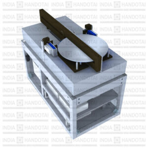
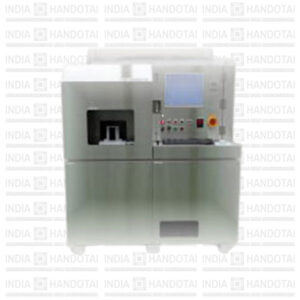
The MX7018 is designed to control thickness, flatness (TTV), warp, waviness and roughness after wire sawing. Capacitive sensors scan a diagonal cut through the center of the wafer. On the sides where the saw wire enters and exits, thickness and roughness are measured simultaneously. (The latter with an opto-electronic measuring system.) Available asin-line integrated module or as hand-loaded stand-alone for spot checks. Comes with our powerful MX-NT operating software.
Measurement type
Thickness
YPI – 500 – Inspection system for large glass substrate
Can inspect surface particles for large size glass substrate and film sheet.
Apply to warpage for sample center position with auto focus sensor unit.
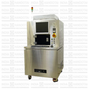
Compact・High performance Wafer surface inspection system
New designed compact and high performance of wafer surface inspection system is reduced 50% to its footprint compared with previous same kind of product. Despite compact body, the maximum sensitivity is 0.15um on bare silicon, and then it can be easy to move to your designated location with desk.
Can choose the surface isolated function (The function can measure a surface of the transparent wafer without receiving contaminations of a back wafer.) as optional for transparent substrate and wafer. Output is map, histogram, which are saved and displayed to an attached PC.

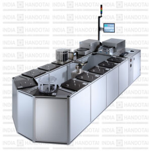
Wafer surface inspection system YPI-N series(Auto loading)
Can scan particles on mirror wafer (silicon wafer) with fast.
Wide range measurement from small size wafer (2/3inch) to 8inch wafer.
YPI – N – XY/YPI – N – Θ
Wafer surface inspection system YPI-N series(Manual)
Can scan particles on mirror wafer (silicon wafer) with fast.
Wide range measurement from small size wafer (2/3inch) to 8inch wafer.
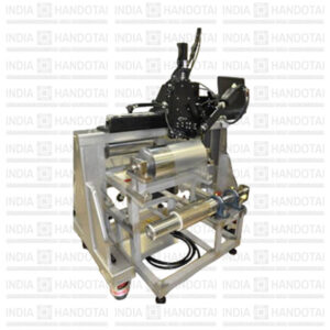
Inspection system for film sheet which can be applied to roll to roll.
YPI-MX-XYA/YPI-MX-ΘA
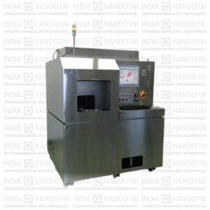
Glass substrate/ Sapphire wafer surface inspection system.
YPI-MX series(Auto loading type)
Specialized to tune for a transparent substrate. Apply to measure a rough polishing of back of substrate.
YPI-MX-XY/YPI-MX-Θ
Glass substrate/ Sapphire wafer surface inspection system
YPI-MX series(Manual)
Specialized to tune for a transparent substrate. Apply to measure a rough polishing of back of substrate.
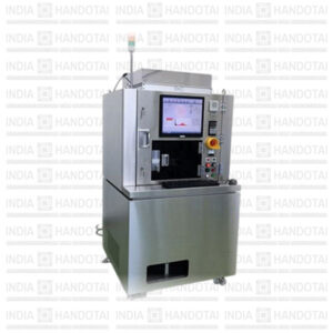
New designed detection units which are cross setting with dual 355nm (UV) laser.
The dual detector contributes enhanced detection for a slight scratch generated directional light scattered compared with conventional particle inspection system.
And also, 355nm laser is effective for isolated detection of SiC surface only.
Inspection time is within 5min for 4inch SiC wafer.